- 您现在的位置:买卖IC网 > Sheet目录310 > AOZ1935QI (Alpha & Omega Semiconductor Inc)IC LED DRVR WHITE BCKLGT 16QFN
AOZ1935
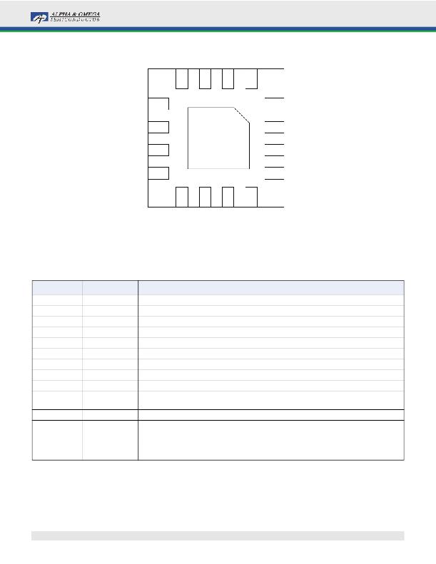
Pin Configuration
VIN
AVCC PGND PGND
13
14
15
16
OV
VOUT
12
11
1
2
LX
LX
PAD
S1
S2
10
9
3
4
PWM
NC
8
S3*
7
GND
6
EN
5
NC
3x3 QFN-16
(Bottom View)
Pin Description
Pin Number
1, 2
3
4, 5
6
7
8
9
10
11
12
13
14
15, 16
PAD
Pin Name
LX
PWM
NC
EN
GND
S3*
S2
S1
VOUT
OV
VIN
AVCC
PGND
Pin Function
Switching node of the step-up converter
Pulse width controlled dimming input. Connect this pin to AVCC when not used
Not internally connected
IC enable
Analog Ground pin
Regulated output current sink #3*
Regulated output current sink #2
Regulated output current sink #1
Output voltage sense pin
Over voltage feedback sense pin. Programmable with a resistor divider, this pin has an
internal 1.2V threshold
Boost converter power supply’s input voltage sense pin
Input supply pin for the IC
Power Ground pin
Exposed Backside Paddle. Connect to ground for electrical and thermal usage. PAD is
internally connected to Analog Ground pin.
*S3 is only for the AOZ1935.
Rev. 1.2 June 2013
www.aosmd.com
Page 3 of 15
发布紧急采购,3分钟左右您将得到回复。
相关PDF资料
AOZ1977AI
IC LED DRVR BCKLGT 16SOIC
AP-104-NT
12V PLUG TRANSFORMER EMPTY CASE
AP-120
PLUG AUTO LOCKING BLACK
AP-121
PLUG AUTO LOCKING BLACK W/LED
AP-124
12V AUTO PLUG STD EURO CE
AP-129
PLUG 12V AUTO EURO CE
AP-130
PLUG 12V AUTO LED SW FUSE CE
AP-131
PLUG 12V AUTO MINI FUSE CE
相关代理商/技术参数
AOZ1948AI
制造商:Alpha & Omega Semiconductor 功能描述:IC LED DRVR BUCK CC SO8
AOZ1950
制造商:AOSMD 制造商全称:Alpha & Omega Semiconductors 功能描述:Boost Regulator White LED Driver
AOZ1950DI
功能描述:IC LED DRVR WHITE BCKLGT 10DFN RoHS:是 类别:集成电路 (IC) >> PMIC - LED 驱动器 系列:EZBoost™ 产品培训模块:Lead (SnPb) Finish for COTS
Obsolescence Mitigation Program 标准包装:2,500 系列:- 恒定电流:- 恒定电压:- 拓扑:升压(升压),切换式电容器(充电泵) 输出数:1 内部驱动器:是 类型 - 主要:背光 类型 - 次要:白色 LED 频率:625kHz ~ 875kHz 电源电压:2.7 V ~ 5.3 V 输出电压:5V 安装类型:表面贴装 封装/外壳:10-TFSOP,10-MSOP(0.118",3.00mm 宽) 供应商设备封装:10-µMAX 包装:带卷 (TR) 工作温度:-40°C ~ 85°C
AOZ1960
制造商:AOSMD 制造商全称:Alpha & Omega Semiconductors 功能描述:Multi-String Boost White LED Driver
AOZ1960DI
功能描述:IC LED DRVR WHITE BCKLGT 24DFN RoHS:是 类别:集成电路 (IC) >> PMIC - LED 驱动器 系列:EZBoost™ 产品培训模块:Lead (SnPb) Finish for COTS
Obsolescence Mitigation Program 标准包装:2,500 系列:- 恒定电流:- 恒定电压:- 拓扑:升压(升压),切换式电容器(充电泵) 输出数:1 内部驱动器:是 类型 - 主要:背光 类型 - 次要:白色 LED 频率:625kHz ~ 875kHz 电源电压:2.7 V ~ 5.3 V 输出电压:5V 安装类型:表面贴装 封装/外壳:10-TFSOP,10-MSOP(0.118",3.00mm 宽) 供应商设备封装:10-µMAX 包装:带卷 (TR) 工作温度:-40°C ~ 85°C
AOZ1977
制造商:AOSMD 制造商全称:Alpha & Omega Semiconductors 功能描述:High Voltage LED Driver IC
AOZ1977-1
制造商:AOSMD 制造商全称:Alpha & Omega Semiconductors 功能描述:High Voltage LED Driver IC
AOZ1977AI
功能描述:IC LED DRVR BCKLGT 16SOIC RoHS:是 类别:集成电路 (IC) >> PMIC - LED 驱动器 系列:EZBoost™ 产品培训模块:Lead (SnPb) Finish for COTS
Obsolescence Mitigation Program 标准包装:2,500 系列:- 恒定电流:- 恒定电压:- 拓扑:升压(升压),切换式电容器(充电泵) 输出数:1 内部驱动器:是 类型 - 主要:背光 类型 - 次要:白色 LED 频率:625kHz ~ 875kHz 电源电压:2.7 V ~ 5.3 V 输出电压:5V 安装类型:表面贴装 封装/外壳:10-TFSOP,10-MSOP(0.118",3.00mm 宽) 供应商设备封装:10-µMAX 包装:带卷 (TR) 工作温度:-40°C ~ 85°C
